
Laser Marking in Electronics
UV and fiber laser marking with the MPERIA® system - maximum precision, minimal heat and maximum speed. Ideal for electronics and microelectronics.
Precise laser marking for electronics & Microelectronics
In electronics and microelectronics manufacturing, the highest precision, minimal thermal stress and maximum process speed are crucial. Components are getting smaller and materials more complex – at the same time, the requirements for traceability, quality assurance and automation are increasing.
Request a free sample label on your original material now – for maximum security in your decision.
The advantages at a glance
High-contrast & precise marking
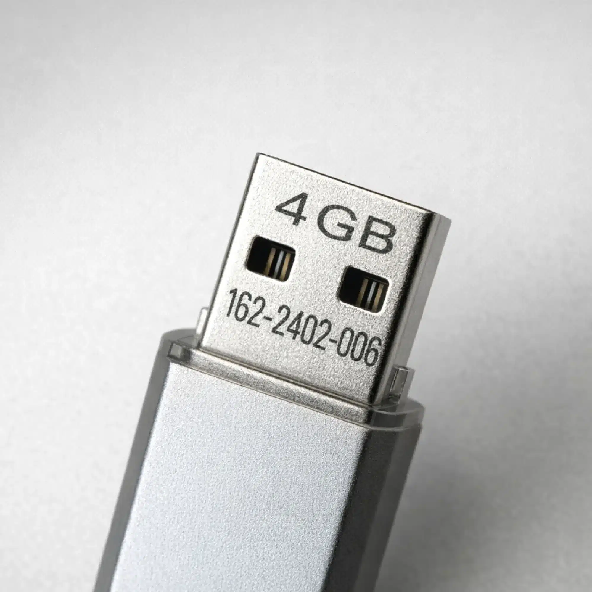
Thanks to minimal focus size and optimized wavelengths, UV and fiber lasers produce pin-sharp markings, micro-fonts and 2D codes. Even on high-density PCBs and the smallest electronic components, the markings remain high-contrast, machine-readable and free of thermal damage.
Reliable 24/7 operation
The MPERIA® UV and fiber laser systems have a sealed laser source with minimal wear. They are designed for continuous operation and ensure high uptime with minimal maintenance.
High speed capability – for automated lines
Laser marking is designed for high cycle rates and can be seamlessly integrated into automated electronics and microelectronics lines. UV and fiber lasers enable fast, reproducible marking in real time – even at high throughputs and dynamic data.
Ideal for cleanroom & microelectronics processes
Particle and residue-free laser marking is predestined for sensitive electronics and microelectronics production such as clean rooms, semiconductor and printed circuit board production.
Abrasion-resistant & durable markings
Laser marking is resistant to abrasion, cleaning and soldering processes. This means that it reliably meets the high quality and durability requirements of electronics and microelectronics production.
Reduced operating costs (TCO)
The elimination of consumables and the high system availability significantly reduce running costs. At the same time, unplanned downtime due to empty inks, clogged nozzles or material changes is avoided.
Sustainable & emission-free
Without inkjet, chemicals or cooling gasses, the lasers are not only environmentally friendly, but also ideally suited for sensitive electronics and microelectronics processes – clean and process-reliable.
Cold marking process
Due to the virtually no thermal effect of the UV laser, no smoking marks, microcracks or deformations occur – even on extremely sensitive or delicate substrates.
OptiBeam™ Technology
The optional OptiBeam™ technology enables a marking field of up to 1000 x 1000 mm – without compromising on marking quality.
Challenges in Electronics and Microelectronics Labeling
Technically demanding industry for product labeling
Electronics and microelectronics manufacturing places particularly high demands on product labeling. Traceability, process reliability and product quality are top priorities. Electronic components must be clearly marked and also be reliably identifiable throughout their entire life cycle – for example, in order to be able to read serial numbers, batch codes, QR or data matrix codes at any time.
At the same time, many electronic components are difficult to identify: Highly compressed PCBs offer only minimal space for markings, sensitive plastics, coatings or semiconductors are sensitive to thermal influences. Traditional methods quickly reach their limits here: Labels or inkjets are often unsuitable in automated or cleanroom processes, can peel off or leave residue. Mechanical engraving exerts pressure on the component and can affect conductor paths or surface structures. Unsuitable laser technologies can also lead to excessive heat input – with discoloration, traces of smoke or material damage to sensitive electronic components.
Area of deployment
Difficulties:
- Printed circuit boards (PCBs) & assemblies: Precise direct identification of printed circuit boards and assemblies with serial numbers, QR or DataMatrix codes – high-contrast, permanently legible and without affecting circuit board paths or solder resists.
- Semiconductors & microcomponents: Micro-labeling of chips, ICs and semiconductor components with the smallest codes and plain text – material-friendly, high-resolution and suitable for highly compacted structures.
- Metal & Hybrid Connectors: High-speed marking of connectors and contact parts made of metal or hybrid materials – abrasion-resistant, process-reliable and ideal for automated series production.
- Electronics housing & consumer electronics: Non-contact laser marking of plastic and metal housings with serial numbers, type plates, CE or RoHS markings – permanent, clean and without additives.
Consequences
UV and fiber lasers can be used to address these challenges in a targeted manner: material-friendly, highly precise, capable of high speeds and fully integrable in automated production lines.
Sample Marking
We look forward to hearing from you
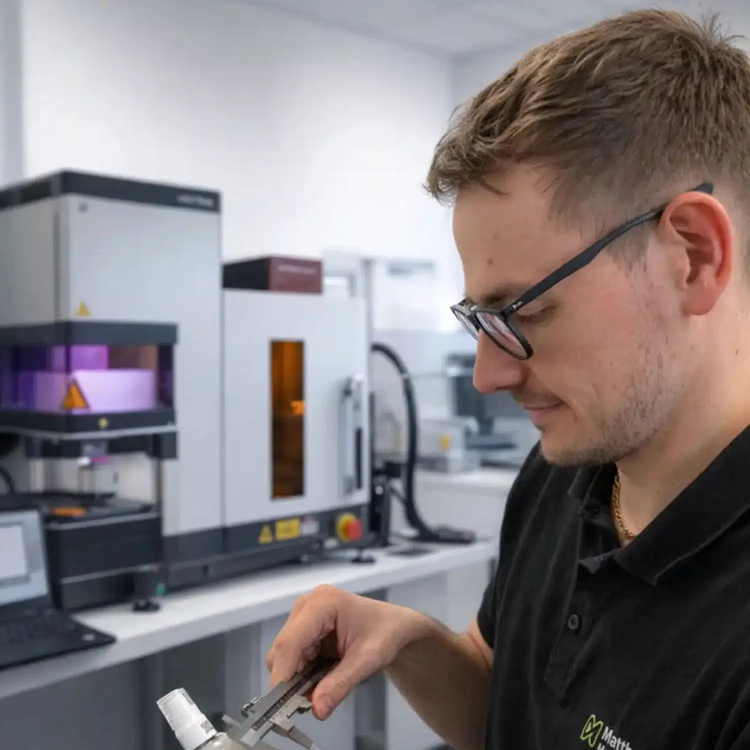
1. Contact & Initial Assessment: Tell us about your application, material, component, or packaging through our contact form. Our laser experts will review your requirements and evaluate feasibility. 2. Personal Feedback & Free Sample Marking: Within 24 hours, you'll receive an initial assessment or follow-up questions. If desired, we'll provide a free sample marking on your original material, including technical evaluation and optional readability testing. 3. Review & Next Steps: Together, we'll discuss suitable solutions, integration options, and the best next steps for your project.


Contact a Laser Expert
Our experts are available to assure that your next printing solution maximizes efficiency, enhances quality, and limits downtime. Contact us to get a quote, request samples, schedule a demonstration, or receive additional product information.